- 您现在的位置:买卖IC网 > Sheet目录2003 > LTC1409IG#TR (Linear Technology)IC ADC 12BIT 800KSPS SMPL 28SSOP
4
LTC1409
POWER REQUIRE E TS
W U
(Note 5)
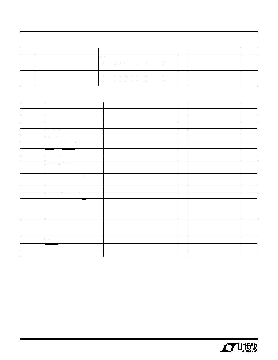
TI I G CHARACTERISTICS
W U
SYMBOL
PARAMETER
CONDITIONS
MIN
TYP
MAX
UNITS
fSAMPLE(MAX)
Maximum Sampling Frequency
q
800
kHz
tCONV
Conversion Time
q
900
1250
ns
tACQ
Acquisition Time
q
150
ns
t1
CS to RD Setup Time
(Notes 9, 10)
q
0ns
t2
CS
↓ to CONVST↓ Setup Time
(Notes 9, 10)
q
10
ns
t3
NAP/SLP
↓ to SHDN↓Setup Time
(Notes 9, 10)
q
10
ns
t4
SHDN
↑ to CONVST↓ Wake-Up Time (Note 10)
200
ns
t5
CONVST Low Time
(Notes 10, 11)
q
50
ns
t6
CONVST to BUSY Delay
CL = 25pF
10
ns
q
60
ns
t7
Data Ready Before BUSY
↑
20
35
ns
q
15
ns
t8
Delay Between Conversions
(Note 10)
q
40
ns
t9
Wait Time RD
↓ After BUSY↑
q
–5
ns
t10
Data Access Time After RD
↓
CL = 25pF
15
35
ns
q
45
ns
CL = 100pF
20
45
ns
q
60
ns
t11
Bus Relinquish Time
830
ns
0
°C ≤ TA ≤ 70°C
q
35
ns
–40
°C ≤ TA ≤ 85°C
q
40
ns
t12
RD Low Time
q
t10
ns
t13
CONVST High Time
q
50
ns
t14
Aperture Delay of Sample-and-Hold
– 1.5
ns
Note 5: VDD = 5V, fSAMPLE = 800kHz, tr = tf = 5ns unless otherwise
specified.
Note 6: Linearity, offset and full-scale specifications apply for a single-
ended +AIN input with –AIN grounded.
Note 7: Integral nonlinearity is defined as the deviation of a code from a
straight line passing through the actual endpoints of the transfer curve.
The deviation is measured from the center of the quantization band.
Note 8: Bipolar offset is the offset voltage measured from – 0.5LSB when
the output code flickers between 0000 0000 0000 and 1111 1111 1111.
Note 9: Guaranteed by design, not subject to test.
Note 10: Recommended operating conditions.
The q indicates specifications which apply over the full operating
temperature range; all other limits and typicals TA = 25°C.
Note 1: Absolute Maximum Ratings are those values beyond which the life
of a device may be impaired.
Note 2: All voltage values are with respect to ground with DGND and
AGND wired together (unless otherwise noted).
Note 3: When these pin voltages are taken below VSS or above VDD, they
will be clamped by internal diodes. This product can handle input currents
greater than 100mA below VSS or above VDD without latch-up.
Note 4: When these pin voltages are taken below VSS they will be clamped
by internal diodes. This product can handle input currents greater than
100mA below VSS without latchup. These pins are not clamped to VDD.
(Note 5)
SYMBOL
PARAMETER
CONDITIONS
MIN
TYP
MAX
UNITS
ISS
Negative Supply Current
CS High
q
10
15
mA
Nap Mode
CONVST = CS = RD = SHDN = 0V, NAP/SLP = 5V
10
A
Sleep Mode
CONVST = CS = RD = SHDN = 0V, NAP/SLP = 0V
1
A
PDISS
Power Dissipation
q
80
120
mW
Nap Mode
CONVST = CS = RD = SHDN = 0V, NAP/SLP = 5V
3.8
6
mW
Sleep Mode
CONVST = CS = RD = SHDN = 0V, NAP/SLP = 0V
0.01
mW
发布紧急采购,3分钟左右您将得到回复。
相关PDF资料
LTC1410IG#TR
IC ADC 12BIT 1.25MSPS SMP 28SSOP
LTC1411IG#TRPBF
IC A/D CONV 14BIT 2.5MSPS 36SSOP
LTC1412IG#TR
IC ADC 12BIT 3MSPS SAMPLE 28SSOP
LTC1414IGN#TRPBF
IC A/D CONV 14BIT SAMPLNG 28SSOP
LTC1415CG#TRPBF
IC A/D CONV 12BIT SAMPLNG 28SSOP
LTC1416IG#TR
IC ADC 14BIT 400KSPS SMPL 28SSOP
LTC1417AIGN#TR
IC ADC 14BIT 400KSPS SMPL 16SSOP
LTC1418ACG#TRPBF
IC A/D CONV 14BIT SRL&PAR 28SSOP
相关代理商/技术参数
LTC1409IG#TRPBF
功能描述:IC A/D CONV 12BIT SAMPLNG 28SSOP RoHS:是 类别:集成电路 (IC) >> 数据采集 - 模数转换器 系列:- 标准包装:1,000 系列:- 位数:12 采样率(每秒):300k 数据接口:并联 转换器数目:1 功率耗散(最大):75mW 电压电源:单电源 工作温度:0°C ~ 70°C 安装类型:表面贴装 封装/外壳:24-SOIC(0.295",7.50mm 宽) 供应商设备封装:24-SOIC 包装:带卷 (TR) 输入数目和类型:1 个单端,单极;1 个单端,双极
LTC1409ISW
功能描述:IC A/D CONV 12BIT SAMPLNG 28SOIC RoHS:否 类别:集成电路 (IC) >> 数据采集 - 模数转换器 系列:- 标准包装:1,000 系列:- 位数:12 采样率(每秒):300k 数据接口:并联 转换器数目:1 功率耗散(最大):75mW 电压电源:单电源 工作温度:0°C ~ 70°C 安装类型:表面贴装 封装/外壳:24-SOIC(0.295",7.50mm 宽) 供应商设备封装:24-SOIC 包装:带卷 (TR) 输入数目和类型:1 个单端,单极;1 个单端,双极
LTC1409ISW#PBF
功能描述:IC A/D CONV 12BIT SAMPLNG 28SOIC RoHS:是 类别:集成电路 (IC) >> 数据采集 - 模数转换器 系列:- 标准包装:1,000 系列:- 位数:12 采样率(每秒):300k 数据接口:并联 转换器数目:1 功率耗散(最大):75mW 电压电源:单电源 工作温度:0°C ~ 70°C 安装类型:表面贴装 封装/外壳:24-SOIC(0.295",7.50mm 宽) 供应商设备封装:24-SOIC 包装:带卷 (TR) 输入数目和类型:1 个单端,单极;1 个单端,双极
LTC1409ISW#TR
功能描述:IC ADC 12BIT 800KSPS SMPL 28SOIC RoHS:否 类别:集成电路 (IC) >> 数据采集 - 模数转换器 系列:- 标准包装:1,000 系列:- 位数:12 采样率(每秒):300k 数据接口:并联 转换器数目:1 功率耗散(最大):75mW 电压电源:单电源 工作温度:0°C ~ 70°C 安装类型:表面贴装 封装/外壳:24-SOIC(0.295",7.50mm 宽) 供应商设备封装:24-SOIC 包装:带卷 (TR) 输入数目和类型:1 个单端,单极;1 个单端,双极
LTC1409ISW#TRPBF
功能描述:IC A/D CONV 12BIT SAMPLNG 28SOIC RoHS:是 类别:集成电路 (IC) >> 数据采集 - 模数转换器 系列:- 标准包装:1,000 系列:- 位数:12 采样率(每秒):300k 数据接口:并联 转换器数目:1 功率耗散(最大):75mW 电压电源:单电源 工作温度:0°C ~ 70°C 安装类型:表面贴装 封装/外壳:24-SOIC(0.295",7.50mm 宽) 供应商设备封装:24-SOIC 包装:带卷 (TR) 输入数目和类型:1 个单端,单极;1 个单端,双极
LTC1410CG
功能描述:IC A/D CONV 12BIT SAMPLNG 28SSOP RoHS:否 类别:集成电路 (IC) >> 数据采集 - 模数转换器 系列:- 标准包装:1,000 系列:- 位数:12 采样率(每秒):300k 数据接口:并联 转换器数目:1 功率耗散(最大):75mW 电压电源:单电源 工作温度:0°C ~ 70°C 安装类型:表面贴装 封装/外壳:24-SOIC(0.295",7.50mm 宽) 供应商设备封装:24-SOIC 包装:带卷 (TR) 输入数目和类型:1 个单端,单极;1 个单端,双极
LTC1410CG#PBF
功能描述:IC A/D CONV 12BIT SAMPLNG 28SSOP RoHS:是 类别:集成电路 (IC) >> 数据采集 - 模数转换器 系列:- 标准包装:1 系列:microPOWER™ 位数:8 采样率(每秒):1M 数据接口:串行,SPI? 转换器数目:1 功率耗散(最大):- 电压电源:模拟和数字 工作温度:-40°C ~ 125°C 安装类型:表面贴装 封装/外壳:24-VFQFN 裸露焊盘 供应商设备封装:24-VQFN 裸露焊盘(4x4) 包装:Digi-Reel® 输入数目和类型:8 个单端,单极 产品目录页面:892 (CN2011-ZH PDF) 其它名称:296-25851-6
LTC1410CG#TR
功能描述:IC ADC 12BIT 1.25MSPS SMP 28SSOP RoHS:否 类别:集成电路 (IC) >> 数据采集 - 模数转换器 系列:- 标准包装:1,000 系列:- 位数:12 采样率(每秒):300k 数据接口:并联 转换器数目:1 功率耗散(最大):75mW 电压电源:单电源 工作温度:0°C ~ 70°C 安装类型:表面贴装 封装/外壳:24-SOIC(0.295",7.50mm 宽) 供应商设备封装:24-SOIC 包装:带卷 (TR) 输入数目和类型:1 个单端,单极;1 个单端,双极